01
Start with the budget
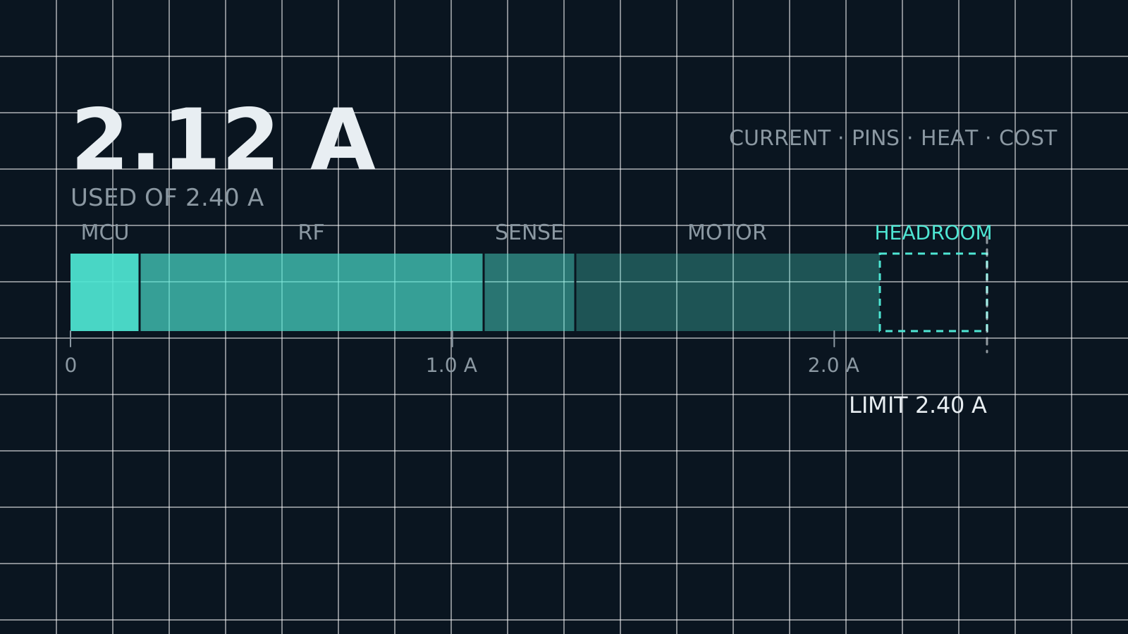
Work out the current, the pins, the heat and the cost first. Choosing parts comes after that, never before.
01 / PRINCIPLEStart with the budget
Topic 04 / The Art of Circuit DesignIn progress
The circuit that works on the bench and the circuit that ships are separated by a few dozen decisions nobody writes down. This is the set I keep coming back to.
Explore the ten principles ↓Current does not read your schematic. It takes the path you actually built.
Work out the current, the pins, the heat and the cost first. Choosing parts comes after that, never before.
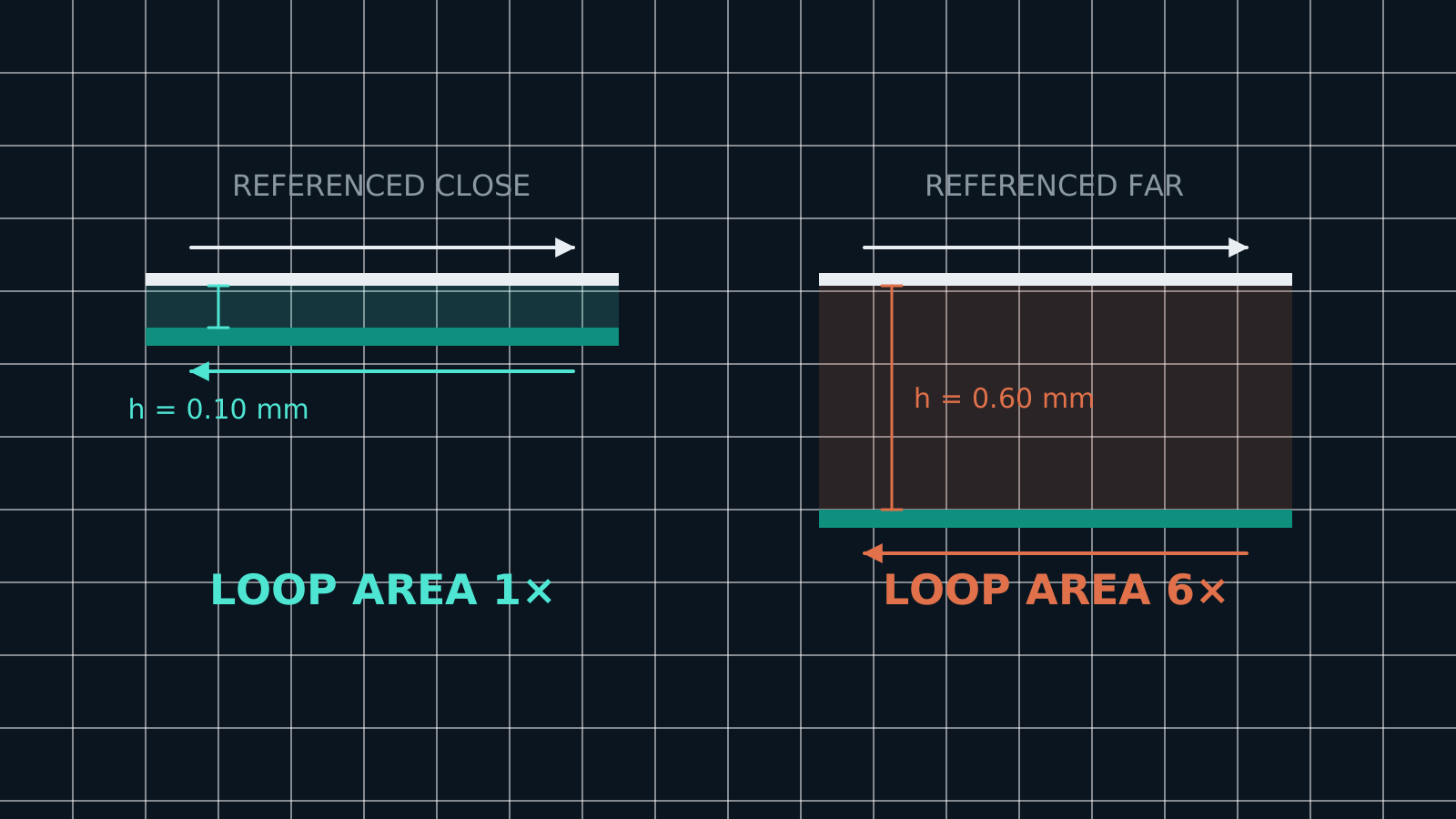
Current that goes out has to come back. If you cannot say where the return path runs, that net is not routed yet.
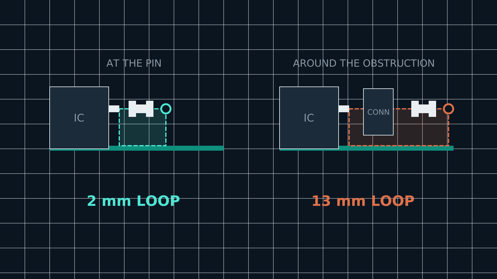
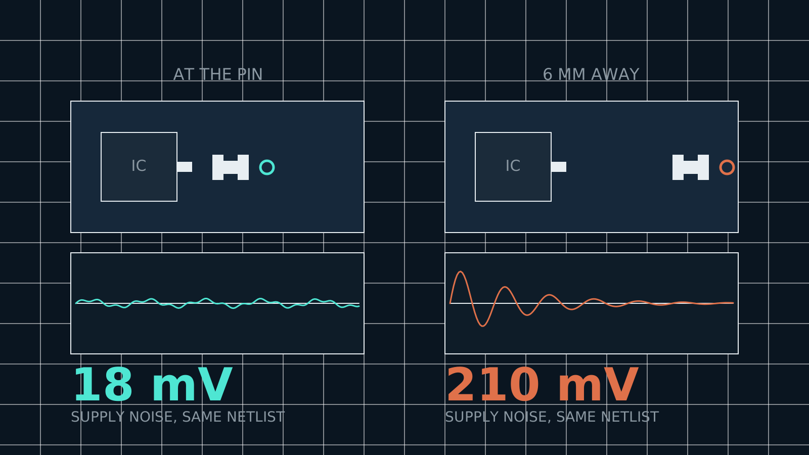
Put the capacitor against the supply pin with its own via beside it — not wherever there happened to be room.
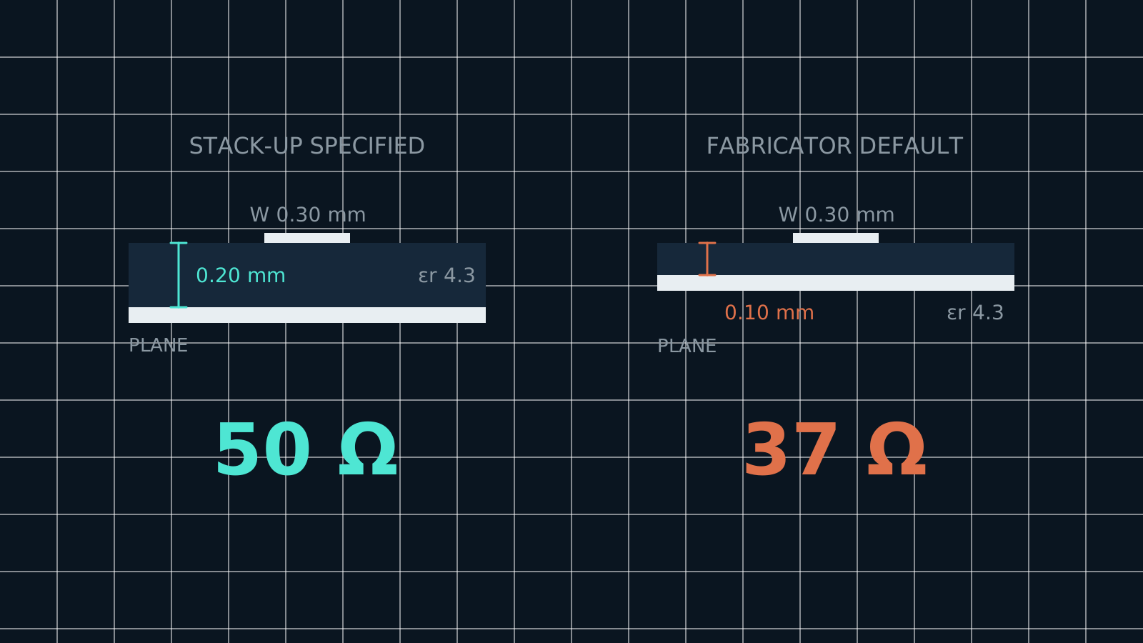
The stack-up is decided before the first trace. It is a design decision, not the fabricator's default.
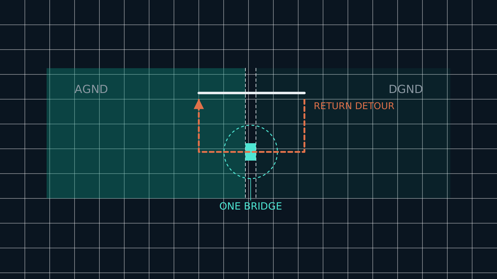
Keep analogue and digital ground apart, then join them at one point you chose on purpose. One point.
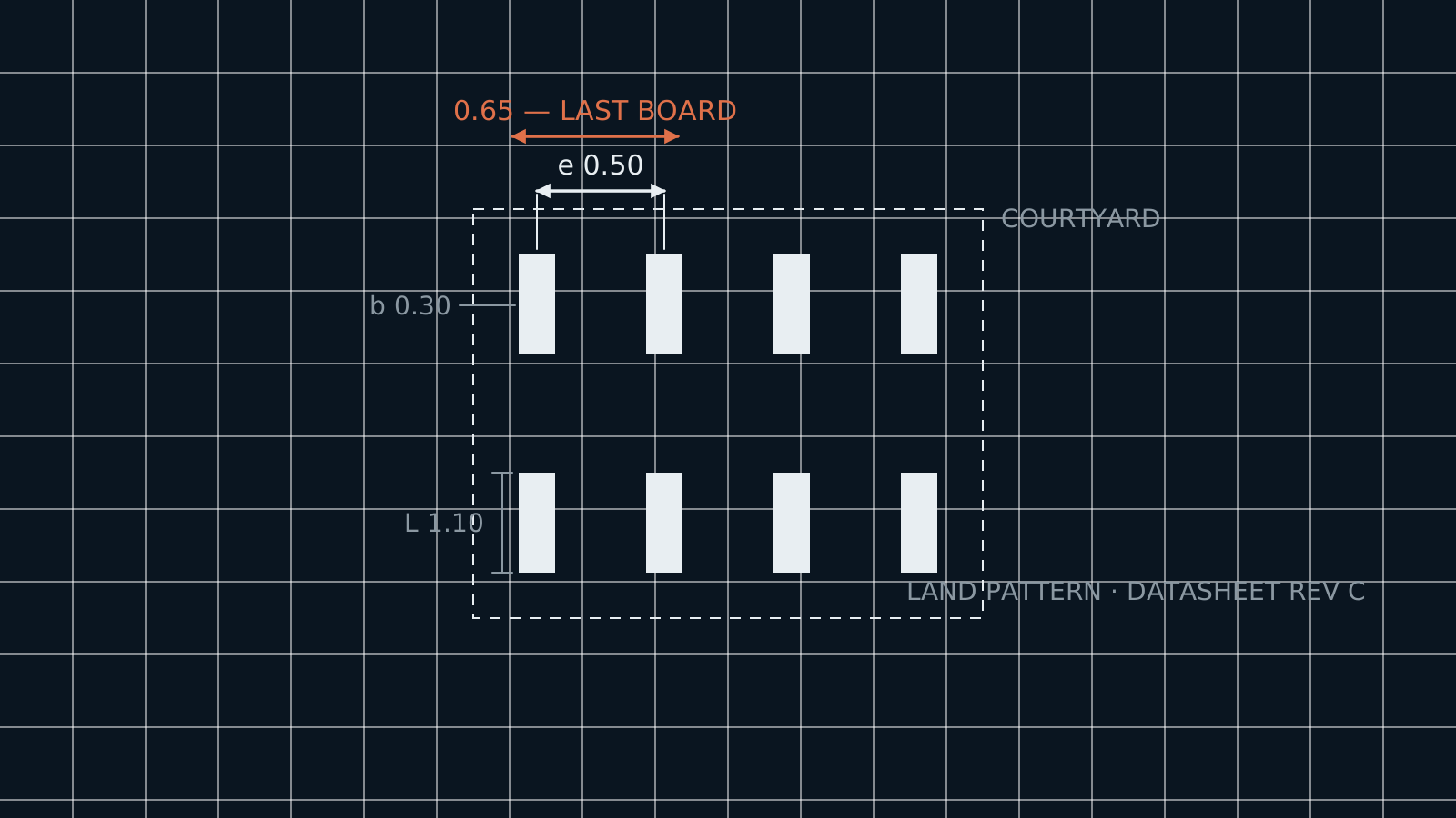
Check a new footprint against the datasheet, not against your last board. Getting it wrong costs the whole batch.
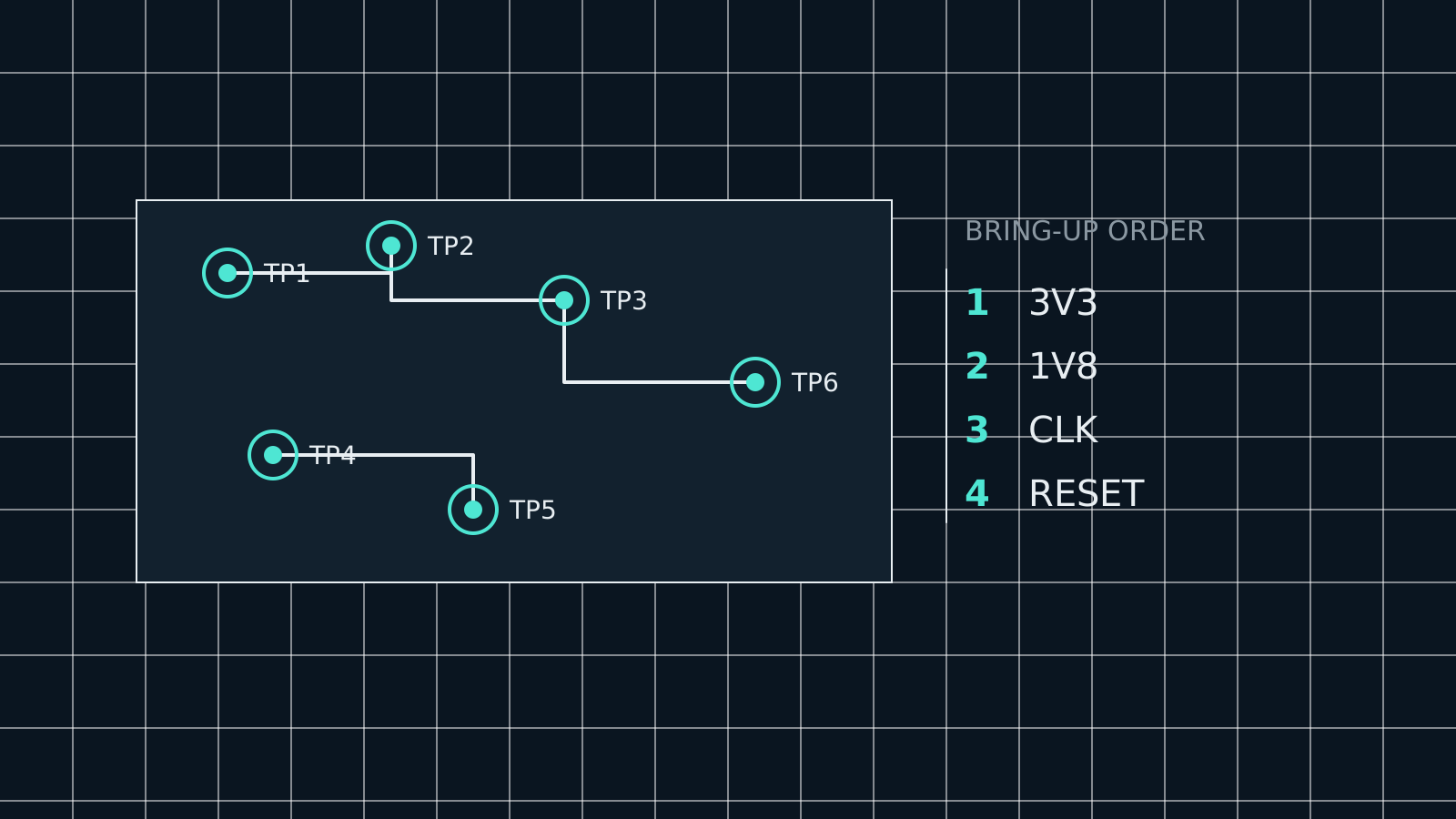
Test points, bring-up order and the jig — decided while the board can still change.
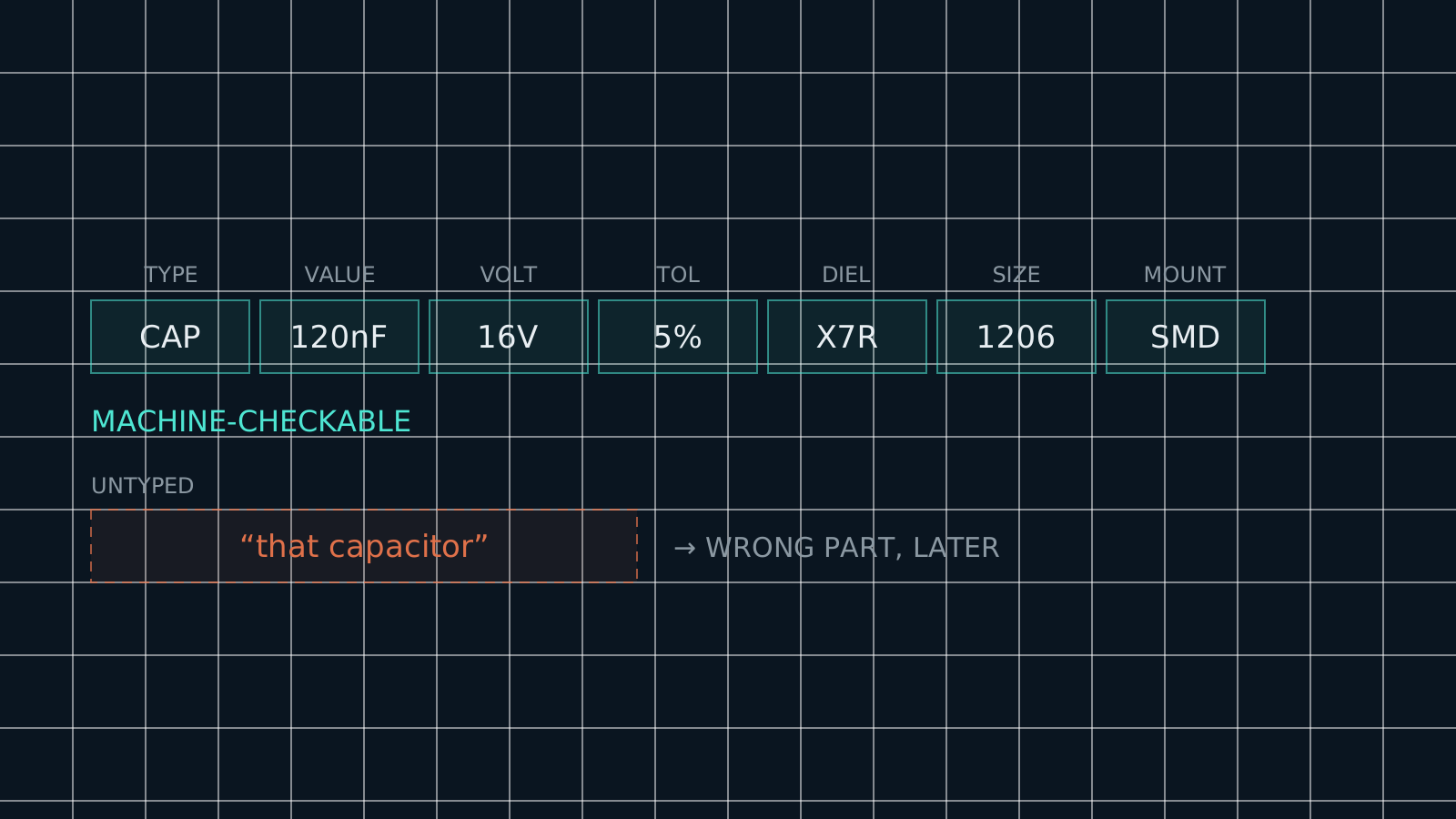
CAP, 120nF, 16V, 5%, X7R, 1206, SMD can be checked by a machine. “that capacitor” becomes a substitution error later.
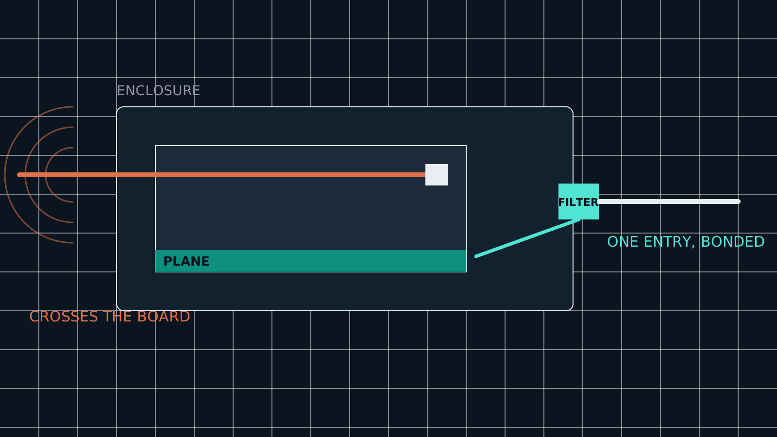
Whether it passes is decided by placement, planes and cable entry — not by a filter added after the pre-scan fails.
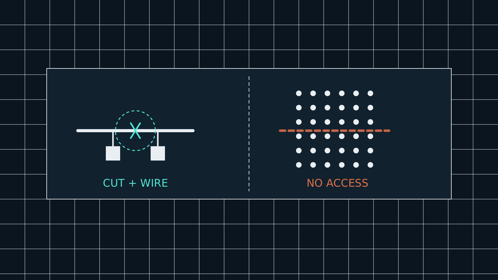
Somebody will cut a trace and add a wire on this board. Make that survivable now, while it is still cheap.
On a schematic the position of a decoupling capacitor means nothing — a schematic has no distance in it. On a board it means everything. Against the supply pin with its own via, or a few millimetres away around an obstruction, are two different products. Same netlist; supply noise an order of magnitude apart.
A trace is only half a circuit. The return current follows the path of least impedance, which at any real frequency means directly under the trace. Put a slot in the plane and it has to detour — and the loop it makes is now an antenna.
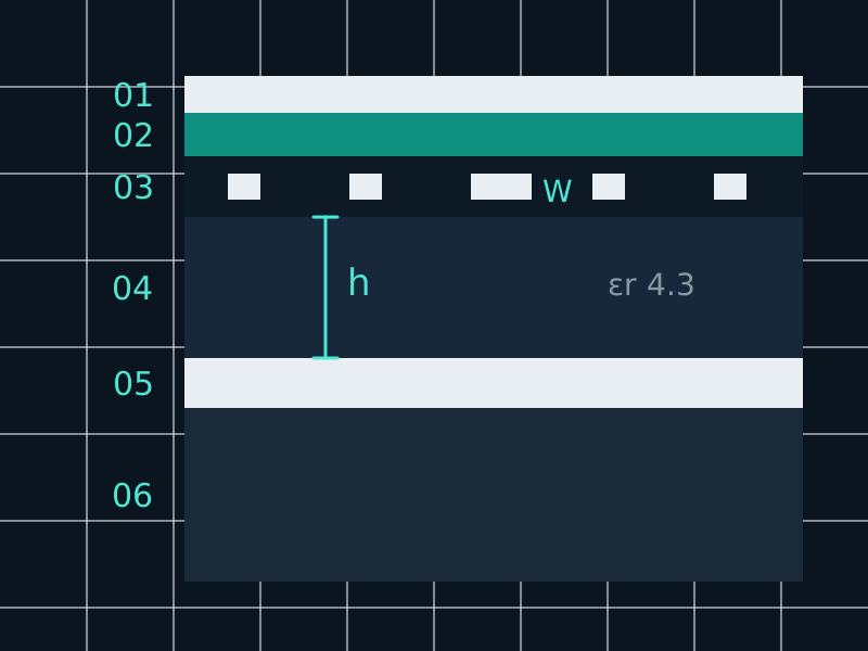
A 50 Ω trace: its width, its distance to the reference plane, and the dielectric in between — decided together, or not decided at all.
For people: polarity, pin one, revision. Assembly and rework both depend on it.
Decides where solder goes and, more importantly, where it does not.
The trace runs here. Its reference plane is the layer directly below.
Dielectric thickness and constant. This is what actually sets the impedance.
Power and ground. The return current for every signal above lives here.
The mechanical spine, and the reference for keeping the stack symmetric.
A parametric part name is a sentence anyone can check and any script can validate. A nickname is a purchasing decision waiting to go wrong at three in the morning during a rush build.
Test points, pin one in the silkscreen, room for a probe, an accessible rework path. The board will be modified — decide now whether that is possible or whether it means scrapping it.
Power budget, pin map, thermal path and the block diagram — before a single component is chosen.
The stack-up and the impedance rules are released with the schematic, not discovered at fabrication.
An informal EMC scan while the design can still move, then formal test and safety on a frozen configuration.
Both produce a working schematic. Only one of them produces a board you can manufacture, test and pass EMC with — and the difference is when you start thinking about the physical.
Placement, stack-up and return paths are considered while the schematic is still soft. The schematic takes longer to freeze and then does not move again — which is the only part of the schedule that actually matters.
Make intelligence useful
Work in progress
Topic 04 / The Art of Circuit Design
This topic is still being written. The structure below is in place, but the copy, figures and examples are not final — so they are blurred for now.